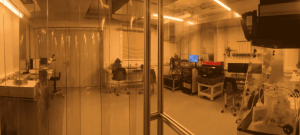
Laboratories
Multiprobe Lab Room CEEC II U0.37 Telephone: +49 3641 9-48741
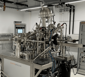
Image: AG TurchaninUltra high vacuum (UHV) Multiprobe System (ScientaOmicron) for analysis of structural, chemical and electronic properties of nanomaterials and sample preparation:
- operating temperature range 50 – 1300 K
- sample preparation by PVD and CVD techniques, Ar+ sputtering
- photoelectron spectroscopy including monochromatic and non-monochromatic XPS (Al Kα, Mg Kα), UPS (e.g., He I), chemical mapping and depth profiling
- scanning probe techniques including variable temperature AFM and STM
- low energy electron diffraction (LEED)
Multiprobe Lab Room CEEC II U0.37 Telephone: +49 3641 9-48741
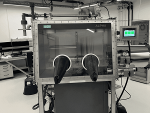
Image: AG TurchaninGlovebox GS Alpha X-Line
Nanosensor Lab Room 258 Telephone: +49 3641 9-48759
Image: Emad NajafidehaghaniHigh vacuum (HV) probe station (Lakeshore) for analysis of electrical properties of nanomaterials and devices:
- Cryogenic vacuum probe station, 4 – 450 K (LakeShore Cryotronics TTPX) for (opto-) electrical characterization in vacuum
- Light sources (Thorlabs LEDs 365 nm and 455 nm, Thorlabs Pigtailed Laser Diodes)
Gas sensing setup
- High vacuum (HV) gas sensing setup
Nanosensor Lab Room 138 Telephone: +49 3641 9-48472
Image: Emad NajafidehaghaniAmbient air probe stations (Signatone) for analysis of electrical properties of nanomaterials and devices:
- Precision LCR meter, 20 Hz - 2 MHz (Keysight E4980A)
- Precision sourcemeters, 1 µA - 200 V and 1 fA - 10 A (Keithley 2614B)
- Perestalitic pump (Spetec Perimax)
- Sampling oscilloscope (GwInstek GDS-1052-U)
Nanosensor Lab Room 138 Telephone: +49 3641 9-48472
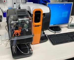
Image: Andrey TurchaninMP-SPR Navi™ 210A VASA
- Automated liquid handling of up to 6- different samples for unattended runs
- Partial loop injections enabling minimized sample consumption
- 4 simultaneous measurements in 2 fluidic channels, two independent wavelength measurements from the same spot, enabling detection of thickness and refractive index or conformation changes
- Exceptionally wide angular range 40˚ - 78˚
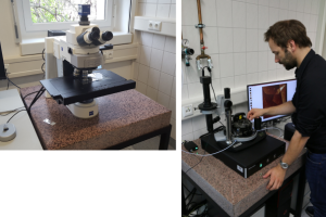
Microscopy Lab Room 255 Telephone: +49 3641 9-48750
Image: AG TurchaninOptical Microscopy (Zeiss), Atomic Force Microscopy (NT MDT):
- AFM (contact and tapping modes) / Lateral Force Microscopy / Phase Imaging/ Force Modulation/ Lithography: AFM (Force)
- STM/ Magnetic Force Microscopy/ Electrostatic Force Microscopy/ Scanning Capacitance Microscopy/ Kelvin Probe Microscopy
- Different Measurement modes (air/inert gas atmosphere/liquids)
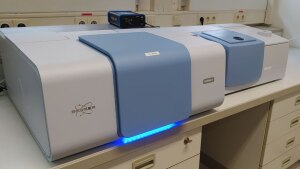
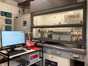
Spectroscopy Lab Room CEEC II U0.22 Telephone: +49 3641 9-48218
Image: AG TurchaninPolarization modulated infrared reflection absorption spectroscopy (PM-IRRAS, Bruker) for the structural and chemical characterization of adsorbed materials on metal surfaces:
- angle of incidence between 70° and 90°
- high-frequency modulation between s- and p-polarization using a PMA 50 photoelastic modulator (ZnSe, 42 kHz, AR-coated); dual channel acquisition for both signals
- mercury cadmium telluride (MCT) detector with non-dichroic BaF2 window
- spectral range 4000 - 750cm-1
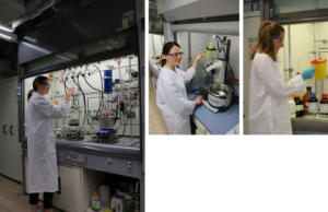
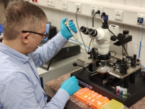
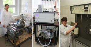
Chemistry Lab Room 253 Telephone: +49 3641 9-48470
Image: AG TurchaninSample preparation and functionalization of 2D materials under ambient and inert conditions:
- Self-assembled monolayer preparation
- Chemical synthesis of target molecules
- Millipore water purification system
- Schlenk technique
- Ar, O2, N2 supply
Chemistry Lab Room 253 Telephone: +49 3641 9-48470
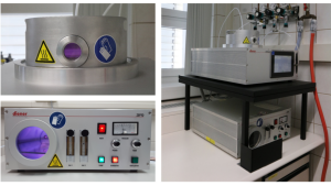
Image: AG TurchaninO+ , air plasma cleaning (ZEPTO, Diener Electronic)
- 40 kHz 0-100 W Generator
Metrohm Autolab
CVD Lab Room 254 Telephone: +49 3641 9-48471
Image: Emad NajafidehaghaniSynthesis of 2D transition-metal dichalcogenides by metalorganic chemical vapor deposition (MOCVD)
- Home-built MOCVD system (Temp: up to 700 °C, Pressure: 10-2 – 103 mbar)
- Mass Spectrometer (1 - 300 amu) for real-time residual gas analysis attached to the MOCVD reactor for understanding the mechanism of the growth process

CVD Lab Room 254 Telephone: +49 3641 9-48471
Image: AG TurchaninSynthesis of 2D transition-metal dichalcogenides by home-built chemical vapor deposition (CVD)
- Three home-built CVD systems: One two-zone and two three-zone furnaces (Ambient and inert conditions)
- Current developed monolayer materials: MoS2, WS2, NbS2, WSe2,MoSe2, NbSe2, MoTe2, 2D lateral heterostructures, wafer-scale MoS2 thin film, etc.
CVD Lab Room 254 Telephone: +49 3641 9-48471
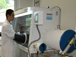
Image: AG TurchaninGlovebox UNIlab M.Braun
- O2 and H2O < 1 ppm
- Can be used with positive and negative pressure
Microfabrication Lab Room 259 Telephone: +49 3641 9-48758
Image: AG Turchanin- CO2 critical point dryer
- Spin coater
- Schlenk technique
- Ar, O2, N2 supply

Microfabrication Lab Room 259 Telephone: +49 3641 9-48758
Image: AG TurchaninNano-Plotter (Gesim NP2.1)
- Non-contact automated nanoliter pipetting for precise liquid handling
- Spotting of liquid microarrays with a resolution down to 20 µm
- Optical target recognition capability down to 50 µm
- Automatic sample aspiration
- Automatic wash and dry stations for piezoelectric micropipettes
- Image analysis of droplet dispensing accuracy via stroboscopic video microscopy
- Humidifier
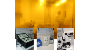
Lithography Lab Room K002 Telephone: +49 3641 9-48473
Image: AG Turchanin- µMLA Tabletop Maskless Aligner (Heidelberg Instruments)Minimum feature sizes of 0.6 µm
- UV LED 365 nm
- Exposure on substrates with dimensions from 5x5mm² to 100x100mm² and a thickness of up to 12mm. Maximum substrate size 6”
- Versatile physical vapor deposition system (Korvus Technology)
- RF magnetron sputtering, e-beam evaporation, thermal evaporation, Organic evaporation
- 6”sample table
- Load-lock fast entry system
- Sample table heating up to 500 °C
- O+ , Ar+ reactive ion etching (ZEPTO RIE, Diener Electronic)
- 13.56 MHz, 0-200 W Generator
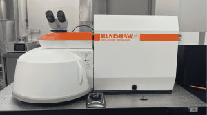
Lithography Lab Room K002 Telephone: +49 3641 9-48473
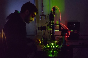
Image: AG TurchaninRenishaw Raman microscope for Raman and photoluminescence measurements using a 532 nm laser
Nanomembrane Lab Room 260 Telephone: +49 3641 9-48751
Image: AG TurchaninElectron beam reactor
- Low Energy Electron (1-500 eV) irradiation of macroscopic samples (up to 4x4 cm2) in High-Vacuum (10-8 mbar)
- Low Energy Electron Beam Lithography with stencil masks
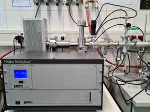
Nanomembrane Lab Room 260 Telephone: +49 3641 9-48751
Image: Vladislav StroganovMass Spectrometer for residual gas analysis
- Designed and sold by Hiden Analytical
- Performs rest gas analysis
- Electron gun ion source, Quadrupole mass analyzer, Faraday cup and electron multiplier detectors
- Sensitivity down to 10-14 mbar
- 9 decades continuous log scale
- Ability to detect external ions
- Possibility to easily modify the "sample" side to fit experimental requirements
- Automated gas sorption analyzer
Nanomembrane Lab Room 260 Telephone: +49 3641 9-48751
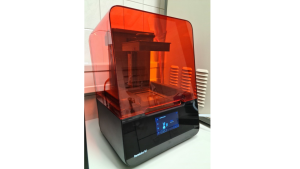
Image: Vladislav Stroganov3D Printer
- Form 3 model from Formlabs
- Utilizes stereolithography (SLA)
- Wide selection of printing materials with different mechanical properties and colors
- Chemically resistant materials are also available
- Build volume dimensions: 145x145x185 mm
- Layer thickness - 25-100 µm
- Minimum reliably printed feature size - 1 mm