Publications 2017
Back Picture of Annalen der Physik Nov 2017
Image: Wiley-VCH: Annalen der PhysikOPEN ACCESS
A. Turchanin
Graphene growth by conversion of aromatic self-assembled monolayers
Annalen der Physik 2017 529, 1700168
DOI: 10.1002/andp.201700168External link
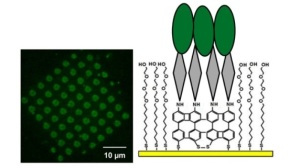
Left:LSM image of VD-Ex based patterned, trisNTA-functionalized sample. Right: Schematic representation of VD patterned, with trisNTA-functionalized SAMs.
Image: ACS Publications: LangmuirL. Kankate, A. Aguf, H. Großmann, M. Schnietz, R. Tampé, A. Turchanin, and A. Gölzhäuser
Vapor phase exchange of self-assembled monolayers for engineering of biofunctional surfaces
Langmuir 2017 33, 3847–3854
DOI: 10.1021/acs.langmuir.6b04207External link
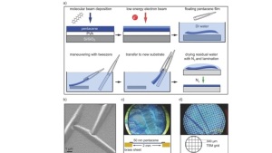
Transfer of thin pentacene films. a) Schematic representation of the transfer method. b) Helium ion microscopy (HIM) image of a crosslinked and transferred 20 nm pentacene film. c) Optical microscopy image of a 50 nm thin pentacene film spanned over a 2 mm hole in a 0.5 mm brass sheet. d) Optical microscopy image of a 50 nm thin pentacene film transferred onto a copper TEM grid (mesh width: 300 µm).
Image: Wiley-VCH: Advanced MaterialsS. J. Noever, M. Eder, F. del Giudice, J. Martin, F. Werkmeister, S. Hallwig, S. Fischer, O. Seeck, N.-E. Weber, C. Liewald, F. Keilmann, A. Turchanin, and B. Nickel
Transferable organic semiconductor nanosheets for application in electronic devices
Advanced Materials 2017 29, 1606283
DOI: 10.1002/adma.201606283External link
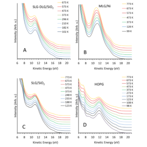
metastable induced electron (MIE) spectra of (A) SLG-DLG/SiO2, (B) MLG/Ni, (C) SLG/SiO2, (D) HOPG.
Image: IOP Publishing: 2d MaterialsOPEN ACCESS
B. A. Chambers, C. Neumann, A. Turchanin, C. T. Gibson, and G. G. Andersson
The direct measurement of the electronic density of states of graphene using metastable induced electron spectroscopy
2D Materials 2017 4, 025068
DOI: 10.1021/acsnano.6b08228External link
Abstract figure of the publication.
Image: ACS Publications: ACS NanoACS Editors Choice
OPEN ACCESS
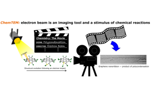
T. W. Chamberlain, J. Biskupek, S. T. Skowron, A. V. Markevich, S. Kurasch, O. Reimer, K. Walker, G. A. Rance, X. Feng, K. Müllen, A. Turchanin, M. A. Lebedeva, A. Majouga, V. G. Nenajdenko, U. Kaiser, E. Besley, and A. N. Khlobystov
Stop-Frame Filming and Discovery of Reactions at the Single-Molecule Level by Transmission Electron Microscopy
ACS Nano 2017 11, 2509–2520
DOI: 10.1021/acsnano.6b08228External link